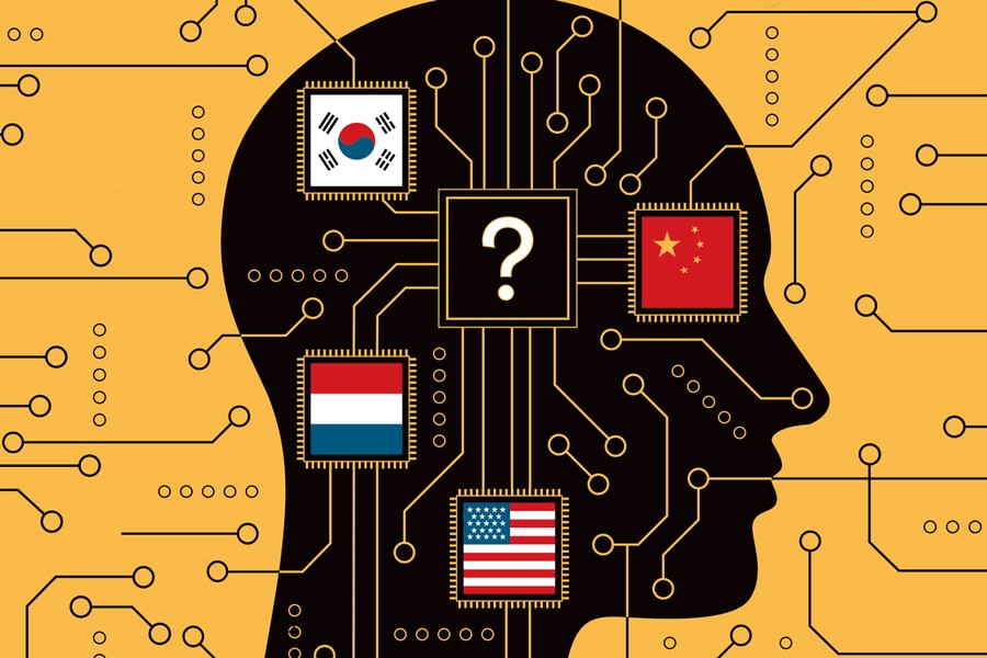
Semiconductors, or ‘chips’, are tiny electronic devices which are the brains of any modern electronic device. Semiconductors are made primarily from silicon or germanium and their manufacture is arguably the most complex process ever mastered by humankind.
During the aerial bombing campaigns of the Second World War, a transition away from mechanical processes was required to increase accuracy, so gears were replaced with electrical charges. The key innovation was the vacuum tube: a metal filament enclosed in glass. Electrical current running through the tube could be switched on or off, with on representing ‘one’ and off representing ‘zero’. Using this binary system of switches, any number could be created and thus the binary code – which remains the foundation of modern computers – was born.
Cutting-edge chips are essential to modern day life and modern militaries, but also essential to facilitating continued progress with technologies such as artificial intelligence (AI).
Vacuum tubes were a step forward, but were unreliable. They were also roughly the size of a fist and so were much too large to be portable. These drawbacks necessitated the eventual move to controlling electrical currents across the surface of silicon. The basic idea of a switch remained, but now these would be created on silicon. These switches were called transistors. The idea of assembling multiple transistors on one piece of silicon then created something called an integrated circuit or ‘chip.’
The final significant innovation I will mention is photolithography – an integral ingredient in the miniaturisation of transistors, and arguably the most complex part of the whole semiconductor supply chain. Originally, the process involved shining light through a mask, which had been cut in the shape of a semiconductor design, at light sensitive material. The light cut many transistors into the silicon, rather than building transistors onto the silicon itself – allowing for much smaller, more detailed designs.
In the infancy of the chip industry, and for much of the 20th century, innovation promulgated from the US defence department and chip production supremacy was retained by the US. Up until the 1980s, companies known as integrated device manufacturers (IDMs), such as Intel, engaged in both design and manufacture of the most cutting-edge semiconductors. Post 1980 though, a new model emerged. In 1985 Morris Chang, formerly a Texas Instruments (TI) executive in the US, was recruited by the Taiwanese government to develop its chip industry. Chang pioneered what is now the foundry business model: focusing solely on manufacturing for other firms which have already designed the chips. This allowed the emergence of ‘fabless’ chip design companies (such as Nvidia), which lack the fabrication plants (or fabs) necessary to produce the chips. Fragmentation of the industry allowed for increasing specialisation and the company which Chang founded, The Taiwanese Semiconductor Manufacturing Company (TSMC), is now the largest and most advanced foundry in the world.
IDMs are still prominent in the industry, however the most advanced chips are more commonly produced within the fabless / foundry model. Under this model, the design process requires two types of company: those that design chips (such as Nvidia and Broadcom) and those that produce the Electronic Design Automation (EDA) software used by chip designers (Cadence, Synopsis and Siemens). Both of these subsectors are still dominated by the US. The US holds c.60% market share in fabless design and holds c.72% of the EDA market. Once a manufacturer has designed its chips using EDA software, it then sends its designs to a foundry for production. Taiwan has a 65% share of overall foundry capacity. At the most advanced level of chip, Taiwan dominates, with c.88% of advanced foundry capacity.
Taiwan is far more strategically important and an invasion of the country would represent one of the greatest threats to global economic stability.
To manufacture chips, TSMC relies on a number of equipment manufacturers. The US holds 42% market share in total equipment manufacturing although photolithography is a notable exception. Extreme ultraviolet (EUV) machines, required for the most advanced chip making, are only currently made by one company in the world – the Dutch firm ASML.
The US dilemma
Cutting-edge chips are essential to modern day life and modern militaries, but also essential to facilitating continued progress with technologies such as artificial intelligence (AI). China is equally ambitious in developing its capabilities in this area as the West. This presents two strategic problems which the US is trying to address. Firstly, if China can develop cutting-edge chips to rival those manufactured in Taiwan, there is nothing to stop it developing defence and intelligence technology with these chips that could pose a threat to the US.
Secondly, arguably the world’s most strategic technology is almost entirely manufactured in a country which the US’s greatest adversary claims as sovereign territory. An invasion of Taiwan risks a decade-long technological set back.
For a historical parallel, we need only look to the Russian invasion of Ukraine. The impact on the world economy was devastating and brought inflation which central bankers are still fretting about two years later. Taiwan is far more strategically important and an invasion of the country would represent one of the greatest threats to global economic stability.
The US began sanctioning China in 2017 and since then several export bans have been levied on critical chip-making equipment and advanced chips.
The US response
The US began sanctioning China in 2017 and since then several export bans have been levied on critical chip-making equipment and advanced chips. The US has also pressured allies with key chip making technologies (e.g. The Netherlands and photolithography technology) to restrict China’s ability to build or access cutting-edge chips. Chinese companies can no longer import Nvidia’s newest AI-focused chip, nor can they order ASML’s EUV machines or use its maintenance services.
Since 2014 China has identified chips as a key technology to produce domestically and has thus poured billions of dollars into domestic manufacturing capacity. China is making a long-term bet on chips and to disregard its efforts would be unwise.
So, in addition to sanctions, the US is aiming to regain a foothold in leading-edge semiconductor manufacturing too, mostly obviously via the 2022 CHIPS Act. The Act appropriates US$53bn for the construction of US-based fabs and chip-making equipment, whilst also funding chip research. A similar European Chips Act was launched in 2022 in Europe.
The future of semiconductors
The CHIPS Act does however come with caveats. Those companies wanting over US$150m in funding are subject to conditions such as stock buyback limitations, preference for union labour and profit sharing. These conditions are likely to make US fabs more uncompetitive with Southeast Asian fabs than they already are. Morris Chang (former CEO of TSMC) estimates US manufacturing costs would be 50% higher than in Taiwan. Leading-edge manufacturers seem unlikely to take up much of the funding and leading-edge production seems unlikely to materially reshore.
Yet sanctions on Chinese domestic production appear more effective. Whilst the release last year by Huawei (a Chinese technology company) of a more-advanced-than-expected chip worried many in Washington, their lack of access to EUV equipment from ASML will limit how much more progress it can make. Overall, the restrictions do look to have strangled Chinese access to semiconductors and stymied leading-edge production for the foreseeable future.
The larger strategic issue is the second detailed above, namely the risk to Taiwan. US protectionism isn’t the panacea, even though it might be a vote winner. The answer more likely lies in diversifying chip sourcing as much as possible. At the leading edge, Samsung is currently the only option, although the proximity of its foundries to North Korea adds another concern. Yet with a combination of onshoring some critical supply and diversifying Southeast Asian partners, the US may be able to reduce dependency. Either way, we expect this to be a key geopolitical theme for many years to come.


